EBSD Phosphor Screen
Introduction
Electron backscatter diffraction (EBSD) is a technique used in the scanning electron microscope (SEM) to collect and explore quantitive microstructure analysis data such as, crystal orientation, phase grain statistics, phase and strain conditions and defects.
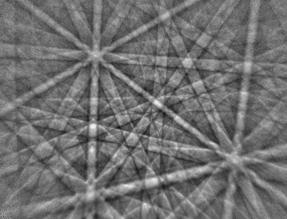
When an electron beam is fired at a prepared crystalline sample, some are absorbed whilst others escape. These escaping electrons may exit near to the Bragg angle and diffract to form Kikuchi bands which correspond to each of the lattice diffracting crystal planes.
These Kikuchi bands are then recorded on the phosphor screen. These patterns are detected by powerful CCD/CMOS sensors which can be automatically analysed and indexed.
EBSD systems usually come in two varieties; one for fast measurements with lower resolution and one for slower, more sensitive work. Modern CMOS EBSD systems are capable of indexing up to 3000 patterns per second.
Why Choose Us?
Analytical Components’ wealth of knowledge and experience has led us to become extremely proficient when it comes to coating phosphor screens used for the EBSD technique. Our unique coating techniques and equipment means we can coat a variety of substrates from float glass to fibre optic plates (FOPS) ranging in sizes from 10-150mm Sq and the equivalent sizes in diameter. Large sizes or uniquely shaped substrates can be provided upon request.
Analytical Components can also supply EBSD screens that are used for in-situ or high-temperature work. Please ask for more details.
EBSD Applications


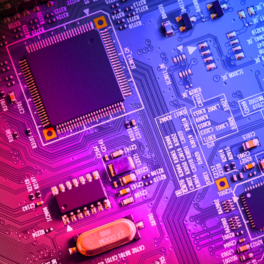
Microelectronics

Metals

Many More Applications
Contact us to find out how EBSD Phosphor Scintillators could work for you and your industry.


